- 您现在的位置:买卖IC网 > Sheet目录1222 > ISL6144EVAL1 (Intersil)EVALUATION BOARD ISL6144 ORING
�� �
�
�ISL6144�
�I� IN1�
�Gate� Fast� Turn-off� Test�
�During� normal� operation,� the� ISL6144� provides� gate� drive�
�voltage� for� the� ORing� MOSFET� when� the� Input� voltage�
�exceeds� the� output� voltage.� The� current� flows� in� the� forward�
�direction� from� the� input� to� the� output.� Now,� what� happens� if�
�the� input� voltage� drops� quickly� below� the� output� voltage� as� a�
�result� of� a� failure� on� the� input� sourcing� power� supply� while�
�the� MOSFET� remained� on?� The� answer� is:� If� the� MOSFET� is�
�kept� on,� current� starts� to� flow� in� the� reverse� direction� from�
�the� output� to� the� input.� Of� course� this� is� not� desired� nor�
�acceptable.� It� will� lead� to� effectively� shorting� the� output� and�
�causing� an� overall� system� failure.� In� order� to� block� this�
�reverse� current,� the� ISL6144� senses� the� voltage� at� both� VIN�
�and� COMP� pins� (this� is� V� OUT� voltage� reduced� by� a� resistor�
�programmable� threshold� (V� TH(HS� ),� it� is� programmed� to�
�55mV� on� the� EVAL� board� and� could� be� adjusted� by�
�changing� R� 1� ,� R� 4� values� for� both� feeds.� If� V� IN� drops� below�
�COMP� (V� OUT� -� V� TH(HS� ),� the� High� Speed� Comparator� turns�
�off� the� gate� of� the� ORing� MOSFET� very� quickly,� the� gate� pull�
�down� current� I� PDH� is� 2A.� As� a� result� the� reverse� current� flow�
�is� prevented.� The� maximum� turn-off� time� is� less� than� 300ns�
�when� using� an� ORing� MOSFET(s)� with� an� equivalent� gate-�
�source� capacitance� of� 39nF� (equivalent� to� Q� TOT� =� 390nC� at�
�V� GS� =� 10V).�
�On� the� ISL6144EVAL1Z� board,� FDB3632� has� an� equivalent�
�t� DELAY(HS)� is� the� High� Speed� Comparator� internal� worst-�
�case� time� delay.� The� setup� in� Figure� 17� can� be� used� to�
�perform� the� Input� dead-short� test;� a� pulse� generator� is�
�connected� between� Gate-Source� of� Q� SHORT1� (use� pulse�
�mode� single� shot,� set� the� frequency� to� <10Hz� and� pulse�
�width� of� approximately� 10ms,� t� RISE� =� 1μs).� Follow� steps� 1�
�through� 5� in� the� two� feed� parallel� operation� section.� Make�
�sure� that� both� feeds� operate� in� parallel� current� sharing�
�mode.� Proceed� with� the� short� test� by� applying� the� single�
�pulse� to� the� gate� of� Q� SHORT1� .� Once� turned� on,� Q� SHORT1�
�shorts� V� IN1� causing� it� to� fall� quickly� (in� less� than� 10� μ� s).�
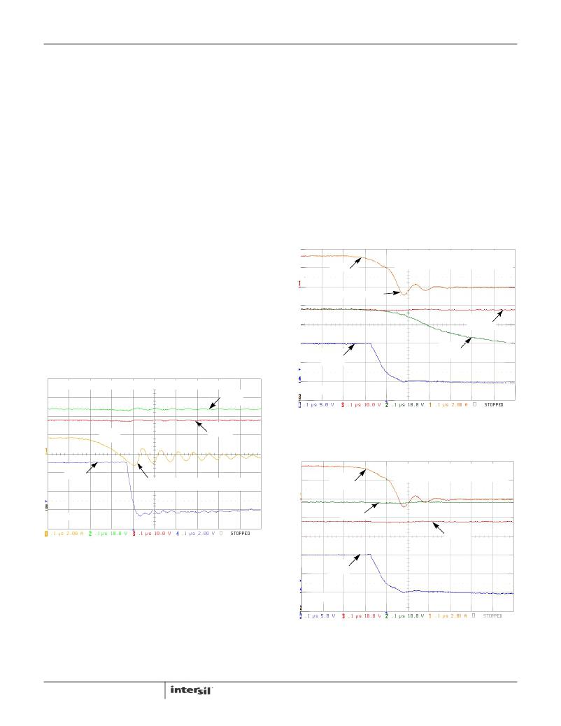
�Figures� 21,� 22� and� 23� show� the� results� for� different�
�combinations� of� C� GS1� and� load� current.� Make� sure� to�
�connect� the� V� IN1� shorting-MOSFET� terminals� as� close� as�
�possible� to� the� V� IN� -GND� (J4� to� J6)� terminals� on� the� EVAL�
�board� to� minimize� lead� impedance� and� reduce� parasitic�
�ringing.�
�V� IN1� =� V� IN2� =� 48V;�
�RESISTIVE� LOAD� =� 6A,� C� gs(ext)� =� 33nF�
�2A/DIV�
�REVERSE CURRENT�
�V� OUT�
�10V/DIV�
�gate-source� capacitance� of� 8.4nF,� some� of� the� tests� are�
�performed� while� an� external� gate� to� source� capacitance� is�
�added� to� demonstrate� gate� current� sink� capability.�
�V� IN1� = V� IN2� = 48V; RESISTIVE LOAD = 4A, C� GS(EXT)� = 0n� F�
�V� G2�
�10V/DIV�
�V� GS1�
�5V/DIV�
�0.1μs/DIV�
�V� IN1�
�10V/DIV�
�I� IN1�
�2A/DIV�
�V� OUT�
�10V/DIV�
�FIGURE� 22.� FAST� SPEED� TURN-OFF� (MOSFET� WITH�
�Q� TOT� =� 8.4nc)� AND� 33nF� EXTERNAL� C� GS�
�V� GS1�
�2V/DIV�
�0.1μs/DIV�
�REVERSE� CURRENT� DISSAPPEARS�
�WHEN� GATE� IS� COMPLETELY� OFF�
�I� IN1�
�2A/DIV�
�V� G2�
�10V/DIV�
�V� IN1� =� V� IN2� =� 48V;�
�RESISTIVE� LOAD� =� 6A,� C� gs(ext)� =� 33nF�
�V� OUT�
�10V/DIV�
�FIGURE� 21.� FAST� SPEED� TURN-OFF�
�(MOSFET� WITH� Q� TOT� =� 8.4nc)�
�Worst-case� turn-off� time� can� be� calculated� as:�
�V� GS1�
�5V/DIV�
�t� toff� (� WC� )� =� t� DELAY� (� HS� )� +� ?� C� GS� -------------� ?�
�t� toff� (� WC� )� =� 50ns� +� ?� 39nF� -----------� ?� =� 284ns�
�?� V� GS� ?�
�?� I� PDH� ?�
�12V�
�?� 2A� ?�
�19�
�(EQ.� 9)�
�0.1μs/DIV�
�FIGURE� 23.� FAST� SPEED� TURN-OFF� (MOSFET� WITH�
�Q� TOT� =� 8.4nc)� AND� 33nF� EXTERNAL� C� gs�
�FN9131.7�
�October� 6,� 2011�
�发布紧急采购,3分钟左右您将得到回复。
相关PDF资料
ISL61853EVAL1Z
EVAL BOARD FOR ISL61853
ISL6227EVAL1
EVALUATION BOARD 1 ISL6227
ISL62386HIEVAL1Z
EVAL BOARD FOR ISL62386HI 32TQFN
ISL6291EVAL1
EVALUATION BOARD FOR ISL6291
ISL6292EVAL2
EVALUATION BOARD 2 ISL6292
ISL6296EVAL1
EVALUATION BOARD 1 ISL6296
ISL6298EVAL1
EVALUATION BOARD 1 ISL6298
ISL6298EVAL2
EVALUATION BOARD 2 ISL6298
相关代理商/技术参数
ISL6144EVAL1Z
功能描述:EVALUATION BOARD ISL6144 ORING RoHS:是 类别:编程器,开发系统 >> 评估演示板和套件 系列:- 标准包装:1 系列:PCI Express® (PCIe) 主要目的:接口,收发器,PCI Express 嵌入式:- 已用 IC / 零件:DS80PCI800 主要属性:- 次要属性:- 已供物品:板
ISL6144IR
功能描述:IC CTRLR MOSFET HV ORING 20-QFN RoHS:否 类别:集成电路 (IC) >> PMIC - O 圈控制器 系列:- 标准包装:1,000 系列:- 应用:电池备份,工业/汽车,大电流开关 FET 型:- 输出数:5 内部开关:是 延迟时间 - 开启:100ns 延迟时间 - 关闭:- 电源电压:3 V ~ 5.5 V 电流 - 电源:250µA 工作温度:0°C ~ 70°C 安装类型:表面贴装 封装/外壳:16-SOIC(0.154",3.90mm 宽) 供应商设备封装:16-SOIC N 包装:带卷 (TR)
ISL6144IR-T
功能描述:IC CTRLR MOSFET HV ORING 20-QFN RoHS:否 类别:集成电路 (IC) >> PMIC - O 圈控制器 系列:- 标准包装:1,000 系列:- 应用:电池备份,工业/汽车,大电流开关 FET 型:- 输出数:5 内部开关:是 延迟时间 - 开启:100ns 延迟时间 - 关闭:- 电源电压:3 V ~ 5.5 V 电流 - 电源:250µA 工作温度:0°C ~ 70°C 安装类型:表面贴装 封装/外壳:16-SOIC(0.154",3.90mm 宽) 供应商设备封装:16-SOIC N 包装:带卷 (TR)
ISL6144IRZA
功能描述:热插拔功率分布 W/ANNEAL 20LD 5X5 QF N ORING FET CONTRLR RoHS:否 制造商:Texas Instruments 产品:Controllers & Switches 电流限制: 电源电压-最大:7 V 电源电压-最小:- 0.3 V 工作温度范围: 功率耗散: 安装风格:SMD/SMT 封装 / 箱体:MSOP-8 封装:Tube
ISL6144IRZA-T
功能描述:IC CTRLR MOSFET HV ORING 20-QFN RoHS:是 类别:集成电路 (IC) >> PMIC - O 圈控制器 系列:- 标准包装:1,000 系列:- 应用:电池备份,工业/汽车,大电流开关 FET 型:- 输出数:5 内部开关:是 延迟时间 - 开启:100ns 延迟时间 - 关闭:- 电源电压:3 V ~ 5.5 V 电流 - 电源:250µA 工作温度:0°C ~ 70°C 安装类型:表面贴装 封装/外壳:16-SOIC(0.154",3.90mm 宽) 供应商设备封装:16-SOIC N 包装:带卷 (TR)
ISL6144IV
功能描述:IC CTRLR MOSFET ORING HV 16TSSOP RoHS:否 类别:集成电路 (IC) >> PMIC - O 圈控制器 系列:- 标准包装:1,000 系列:- 应用:电池备份,工业/汽车,大电流开关 FET 型:- 输出数:5 内部开关:是 延迟时间 - 开启:100ns 延迟时间 - 关闭:- 电源电压:3 V ~ 5.5 V 电流 - 电源:250µA 工作温度:0°C ~ 70°C 安装类型:表面贴装 封装/外壳:16-SOIC(0.154",3.90mm 宽) 供应商设备封装:16-SOIC N 包装:带卷 (TR)
ISL6144IV-T
功能描述:IC CTRLR MOSFET HV ORING 16TSSOP RoHS:否 类别:集成电路 (IC) >> PMIC - O 圈控制器 系列:- 标准包装:1,000 系列:- 应用:电池备份,工业/汽车,大电流开关 FET 型:- 输出数:5 内部开关:是 延迟时间 - 开启:100ns 延迟时间 - 关闭:- 电源电压:3 V ~ 5.5 V 电流 - 电源:250µA 工作温度:0°C ~ 70°C 安装类型:表面贴装 封装/外壳:16-SOIC(0.154",3.90mm 宽) 供应商设备封装:16-SOIC N 包装:带卷 (TR)
ISL6144IVZA
功能描述:IC CTRLR MOSFET ORING HV 16TSSOP RoHS:是 类别:集成电路 (IC) >> PMIC - O 圈控制器 系列:- 标准包装:1,000 系列:- 应用:电池备份,工业/汽车,大电流开关 FET 型:- 输出数:5 内部开关:是 延迟时间 - 开启:100ns 延迟时间 - 关闭:- 电源电压:3 V ~ 5.5 V 电流 - 电源:250µA 工作温度:0°C ~ 70°C 安装类型:表面贴装 封装/外壳:16-SOIC(0.154",3.90mm 宽) 供应商设备封装:16-SOIC N 包装:带卷 (TR)